|
ME405: Mechatronics
Project Documentation and Portfolio by Neil Patel
|


|
|
ME405: Mechatronics
Project Documentation and Portfolio by Neil Patel
|
|
The objective of this lab is to build a simple user interface to facilitate communication between a user and laptop. Further, a digital device will be used to measure analog inputs to examine and visualize how input voltage changes as a function of time. We extended our use of interrupts to examine the voltage response of the Nucleo™ to a button press.
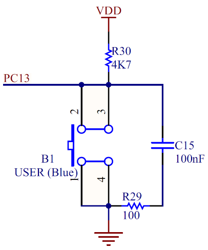
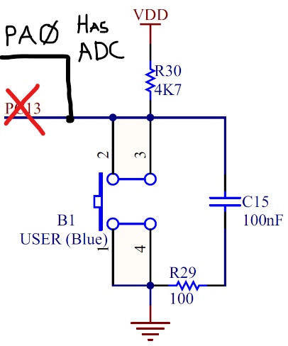
The User button on the Nucleo is connected to PC13, which does not have any ADC input functionality. To combat this issue, we connect a jumper from PC13 to another pin that has ADC functionality (PA0 in this case). The change made to the circuit is illustrated below:
We used an Analog-to-digital converter (ADC) to translate the continuous analog voltage signal into discrete integers using a 3.3 V reference voltage. We used the maximum 12-bit resolution to examine the board's voltage response. Since the User button pin did not have any ADC functionality (as described in the previous section), we had to jumper that pin to another pin designed excclusively for Analog operations. After doing this, we were successfully able to record the ADC readings of the voltage response and store it in a buffer for further use.
To wrap everything together, we implemented Serial Communication using UART to practically create a "virtual handshake" between the front end and the Nucleo™.
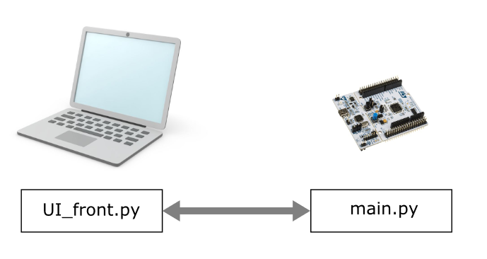
To set up the serial communciation properly, we first created a script that would establish communiations with the Nucleo™. Then we created a script that facilitated the software handshake between the board and the User Interface. After that connection was succesfully made, we focused on capturing the correct data from the ADC and successfully transmitting it over to the front end. Once we successfully transferred the data, we used it to create the best fit plot and a CSV file containing the data.
We were successfully able to derive a plot of values that matched the theoretical description. We accomplished this by finding the buffer in which the greatest change took place by comparing the first and last value. The plot obtained by doing so is displayed below.
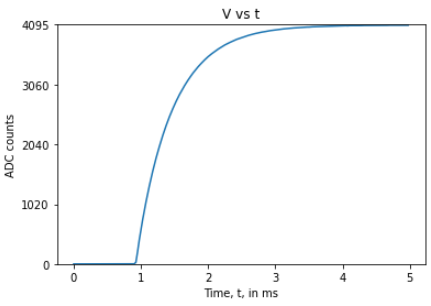
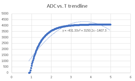
Theoretically, the time constant RC = 0.5 ms. To get the time constant from the plot, we found out the corresponding x value to y = 63.2% of VDD = 2588.04 ADC counts. The time constant using this method came out to be around 0.6 ms, which is fairly close to our theoretical value. The equation and trendline used to calculate this value is shown in the figure below. Notice that the graph below does not consist data points when the ADC count is 0 to make the process of determining time constant easier. Also notice, that the graph has an x-intercept ofaround 1 ms, so that is also taken into consideration when calculating the time constant.
Documentation of this lab can be found here: Lab0x03
A copy of the CSV file of the good step response test can be found here: https://bitbucket.org/npatel68/me405_labs/src/master/lab3/voltvstime.csv
The source code for this lab:
https://bitbucket.org/npatel68/me405_labs/src/master/lab3/UI_front.py
https://bitbucket.org/npatel68/me405_labs/src/master/lab3/main.py